Você está no 3DFinder
Buscamos em Thingiverse, MakerWorld e Printables ao mesmo tempo para te dar o melhor de cada uma.
Descrição
Atomic model for semiconductors
I created this model for my physics students (10th grade) to help understand how silicon semiconductors are build through electron pairs and what doping is. In this model the electrons on inner shells are fixed but those on the outer shell can and must be placed freely. Furthermore the nuclei show the number of protons (ignoring the neutrons).
Parts
- single frames / outer shells for different atoms
- frame with 8 fixed silicon atoms and one free place for different atoms
- three types of atoms: silicon, boron, phosphorus
Usage
1️⃣ Start by showing the three different elements in the single frames, add the missing outer electrons and discuss how the number of electrons equals the number of protons and these atoms are electrically neutral.
2️⃣ Place a silicon atom in the middle of the 3×3 frame.
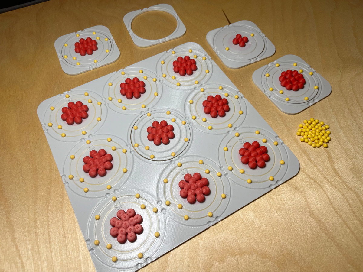
3️⃣ Add the outer electrons and discuss the pair bonding, especially that every silicon atom now “sees” eight outer electrons thus considering the shell as full.
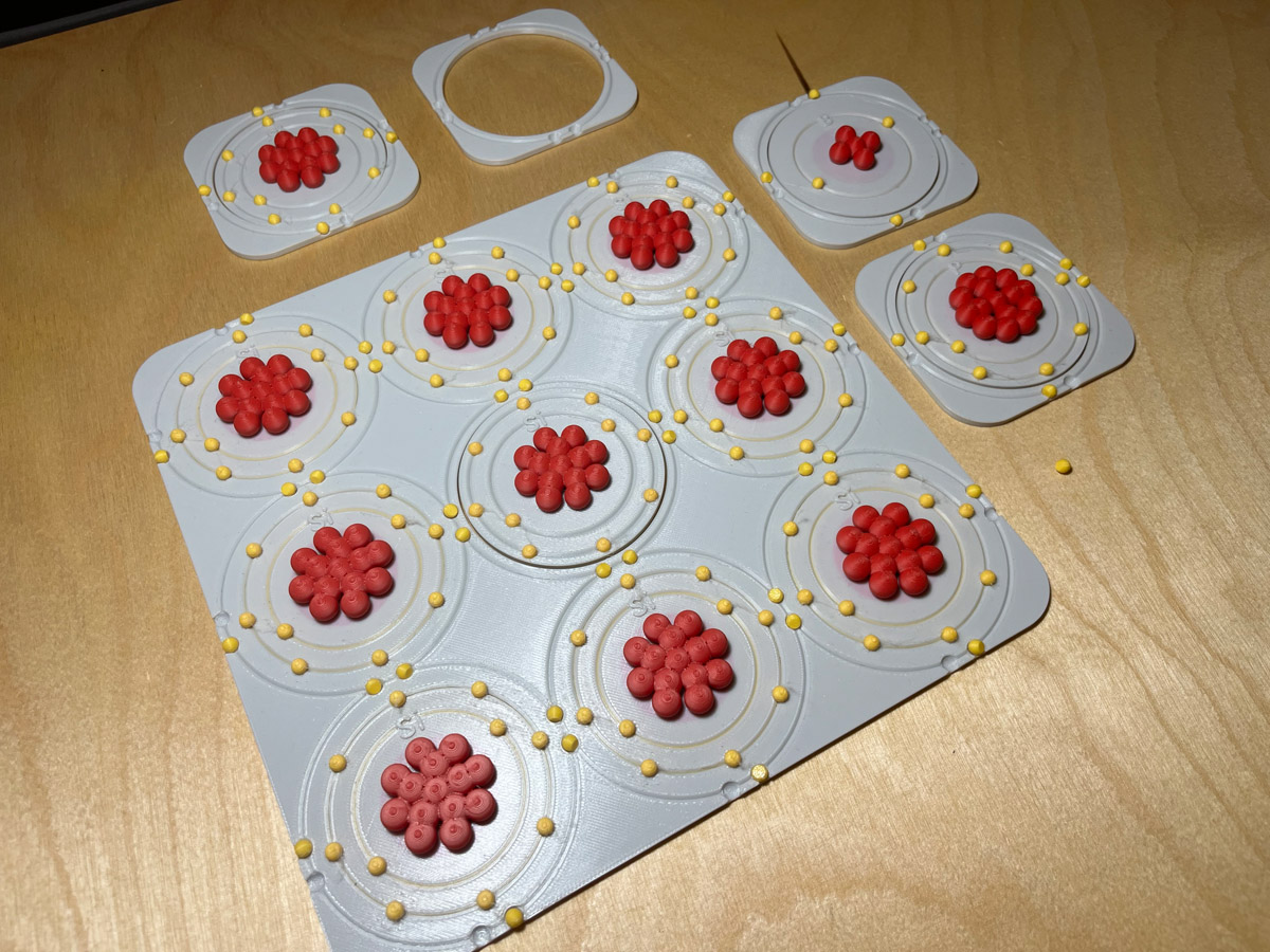
4️⃣ Remove the inner silicon atom and its electrons, discuss that the net charge didn’t change (remover 14 electrons and 14 protons).
5️⃣ p type dopting: now add a boron atom and its electrons in the middle of the grid, discuss again that the net charge remains zero, but now there is one electron missing in the outer shell since boron only has three on its outer shell. Leaving a void.
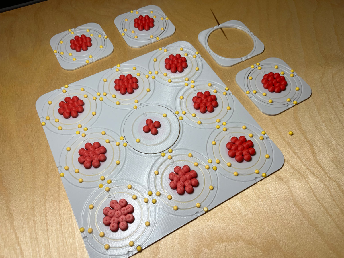
Now move the void by moving some electrons and discuss that local charges appear where the electron of the silicon is gone an filling the void in the boron shell.
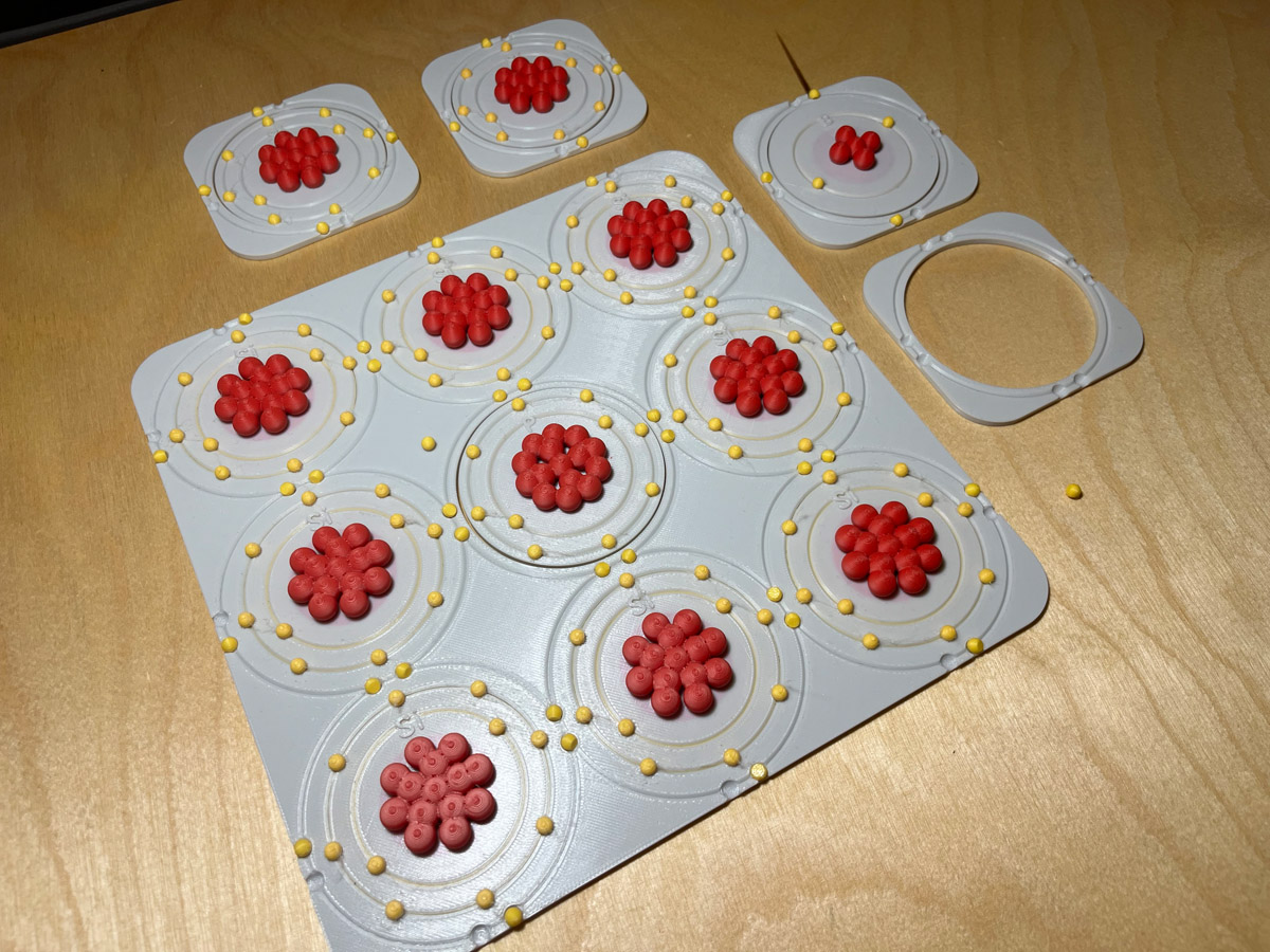
6️⃣ n type doping: add phosphorus and explain the extra electron etc.
Printing
Import the following files as single parts each and color the object appropriately.
- frame.stl + b_protons.stl + b_base.stl + b_electrons.stl
- frame.stl + p_base.stl + p_electrons.stl + p_protons.stl
- frame.stl + si_base.stl + si_electrons.stl + si_protons.stl
- si_multi_base.stl + si_multi_electrons.stl + si_multi_protons.stl
- electron.stl (60 copies)
Print settings:
- multicolor (if possible)
- 0.2mm layer height, 0.4mm nozzle
- 2 walls
- 5 top / 3 bottom shells
- 15% grid infill
- no support
CAD files
You can find my CAD files at onshape and create other atoms etc.

Gostou deste modelo? Crie uma conta grátis para salvar seus favoritos e voltar a eles depois.
Criar conta